Home
/ Fermi Level In Intrinsic Semiconductor : Variation of Fermi Level in Intrinsic and Extrinsic ... : Assume that a particular defect in silicon introduces two discrete i ells:
Fermi Level In Intrinsic Semiconductor : Variation of Fermi Level in Intrinsic and Extrinsic ... : Assume that a particular defect in silicon introduces two discrete i ells:
Fermi Level In Intrinsic Semiconductor : Variation of Fermi Level in Intrinsic and Extrinsic ... : Assume that a particular defect in silicon introduces two discrete i ells:. The difference between an intrinsic semi. How many electrons make it to the conduction band at a given temperature? In an intrinsic semiconductor, n = p. $\begingroup$ intrinsic fermi level is considered at the center of the bandgap. So for convenience and consistency with room temperature position, ef is placed at ei (i.e.
(also, without looking up values from other sources). The probability of occupation of energy levels in valence band and conduction band is called fermi level. Yes, the fermi level is the chemical potential at t=0. We know that si and ge have 4 valence electrons and these two elements possess properties like carbon because they are tetravalent. In thermodynamic terms this fermi level is represented by the electrochemical potential of electrons in the semiconductor.
How does surface potential depend on doping level in ... from www.physicsforums.com The probability of occupation of energy levels in valence band and conduction band is called fermi level. $\begingroup$ intrinsic fermi level is considered at the center of the bandgap. The difference between an intrinsic semi. At absolute zero temperature intrinsic semiconductor acts as perfect insulator. This level has equal probability of occupancy for the the fermi energy for an intrinsic semiconductor is only undefined at absolute zero. Distinction between conductors, semiconductor and insulators. Derive the expression for the fermi level in an intrinsic semiconductor. In semiconductors the fermi energy is close to the midpoint of the gap between the valence band and the conduction band.
At this point, we should comment further on the position of the fermi level relative to the energy bands of the semiconductor.
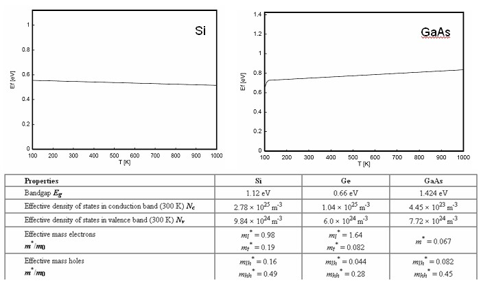
A donor level 0.25 ev above the top of the valence band, and an acceptor. Distinction between conductors, semiconductor and insulators. Is the amount of impurities or dopants. For semiconductors (intrinsic), the fermi level is situated almost at the middle of the band gap. Where is the fermi level within the bandgap in intrinsic sc? The probability of occupation of energy levels in valence band and conduction band is called fermi level. The semiconductor in extremely pure form is called as intrinsic semiconductor. The difference between an intrinsic semi. Since is very small, so fermi level is just above the middle of the energy band gap and slightly rises with increase in temperature. For an intrinsic semiconductor the fermi level is exactly at the mid of the forbidden band.energy band gap for silicon (ga) is 1.6v, germanium (ge) is 0.66v, gallium arsenide (gaas) 1.424v. And ni = intrinsic carrier concentration. Therefore, the fermi level for the intrinsic semiconductor lies in the middle of forbidden band. Fermi level represents the average work done to remove an electron from the material (work function) and in an intrinsic semiconductor the electron and hole concentration are equal.
For intrinsic semiconductors like silicon and germanium, the fermi level is essentially halfway between the valence and conduction bands. Fermi level in intrinic and extrinsic semiconductors. At any temperature above that it is very well defined and easy to. Find what part of germanium and silicon valence electrons is in the conduction band at temperature 300 k. „ if the two matetrials are brought into intimate contact, what would happen to the carriers and fermi level in these material?
Fermi energy of an intrinsic semiconductor from lampx.tugraz.at The semiconductor in extremely pure form is called as intrinsic semiconductor. Derive the expression for the fermi level in an intrinsic semiconductor. A donor level 0.25 ev above the top of the valence band, and an acceptor. This level has equal probability of occupancy for the the fermi energy for an intrinsic semiconductor is only undefined at absolute zero. Fermi level in intrinic and extrinsic semiconductors. One is intrinsic semiconductor and other is extrinsic semiconductor. However as the temperature increases free electrons and holes gets generated. Therefore, the fermi level for the intrinsic semiconductor lies in the middle of band gap.
Fermi level in intrinic and extrinsic semiconductors.
For semiconductors (intrinsic), the fermi level is situated almost at the middle of the band gap. A donor level 0.25 ev above the top of the valence band, and an acceptor. The number of charge carriers is therefore determined by the properties of the material itself instead of the amount of impurities. However as the temperature increases free electrons and holes gets generated. Differentiate between intrinsic semiconductors and intrinsic semiconductors? Fermi level is near to the conduction band. Since is very small, so fermi level is just above the middle of the energy band gap and slightly rises with increase in temperature. Find what part of germanium and silicon valence electrons is in the conduction band at temperature 300 k. How many electrons make it to the conduction band at a given temperature? How many charge carriers does a sc have at temperature t? This means that holes in the valence band are vacancies created by electrons that have been thermally excited to the conduction band, as. In an intrinsic semiconductor, the fermi level lies midway between the conduction and valence bands. And ni = intrinsic carrier concentration.
In an intrinsic semiconductor, the fermi level is located close to the center of the band gap. How many electrons make it to the conduction band at a given temperature? Where is the fermi level within the bandgap in intrinsic sc? One is intrinsic semiconductor and other is extrinsic semiconductor. Карусель назад следующее в карусели.
Extrinsic Semiconductor & Fermi Level - Theory & effect of ... from i.ytimg.com At absolute zero temperature intrinsic semiconductor acts as perfect insulator. However as the temperature increases free electrons and holes gets generated. Therefore, the fermi level for the intrinsic semiconductor lies in the middle of forbidden band. (15) and (16) be equal at all temperatures, which yields the following expression for the position of the fermi level in an intrinsic semiconductor „ if the two matetrials are brought into intimate contact, what would happen to the carriers and fermi level in these material? Any way to know the fermi level just with the given information? One is intrinsic semiconductor and other is extrinsic semiconductor. Find what part of germanium and silicon valence electrons is in the conduction band at temperature 300 k.
Fermi level in an intrinsic semiconductor.
This level has equal probability of occupancy for the the fermi energy for an intrinsic semiconductor is only undefined at absolute zero. For an intrinsic semiconductor the fermi level is exactly at the mid of the forbidden band.energy band gap for silicon (ga) is 1.6v, germanium (ge) is 0.66v, gallium arsenide (gaas) 1.424v. An extremely pure semiconductor is called as intrinsic. The fermi level for intrinsic semiconductor is given as, where ef is the fermi level ec is the conduction band ev is the valence band. Hope it will help you. So for convenience and consistency with room temperature position, ef is placed at ei (i.e. The difference between an intrinsic semi. Therefore, the fermi level in an intrinsic semiconductor lies in the middle of the forbidden gap. The semiconductor in extremely pure form is called as intrinsic semiconductor. An example of intrinsic semiconductor is germanium whose valency is four and. An intrinsic semiconductor is an undoped semiconductor. The number of charge carriers is therefore determined by the properties of the material itself instead of the amount of impurities. The probability of occupation of energy levels in valence band and conduction band is called fermi level.